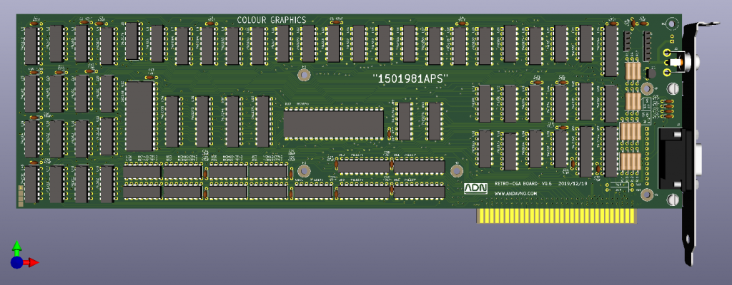
The last post on the Retro-CGA showed the gradual progression from schematic design to board build-up, summarising a period of several busy weeks.
This post acts as a summary of that whole exercise, showing some of the board design detail. More progression is made towards board fabrication and testing.
Features:
It was difficult to convey the detail of the design features of the Retro-CGA board in the last post as I had well and truly run out of steam by the end. Nevertheless, we forge on here now.
One big design detail that I wanted to capture in the Retro-CGA was to have a straight, non re-entrant board edge on the bottom of the card, adjacent to the ISA card edge connector. This design detail would allow for the card to be inserted into a 16-bit ISA socket without fouling, and would also allow for motherboard component clutter adjacent to any 8-bit ISA connector. This detail was achieved after a lot of messing around with the trace routing of the video memory (see photo above).
Another design detail that I wanted to capture was the provision of 0.1″ break-out headers for all of the video output signals. The thinking was that this would make it easier for add-on cards to be attached to the Retro-CGA to achieve additional functionality. For example: an add-on card could be designed to occupy an adjacent ISA slot, directly connected to the Retro-CGA, converting the RGBI video signals into VGA or HDMI.
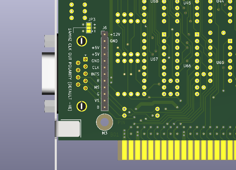
To that end, a 12 pin header was added adjacent to the RGBI port:
The signals presented on this header (J6) are: +12v, +5v, GND, CLK, Red component, Green component, Blue component, Intensity component, Horizontal sync, and Vertical sync. The “CLK” signal is tapped into the local 14MHz clock on the board, so that this clock signal can propagate through the header and into the add-on board if required. The 14MHz signal is not generated on the board itself; it is buffered locally from the ISA connector pin B30. The polarity of the 14MHz clock reference can be chosen with solder jumper JP3 (polarity meaning the phase; clocking on either the rising or falling edge of the signal).
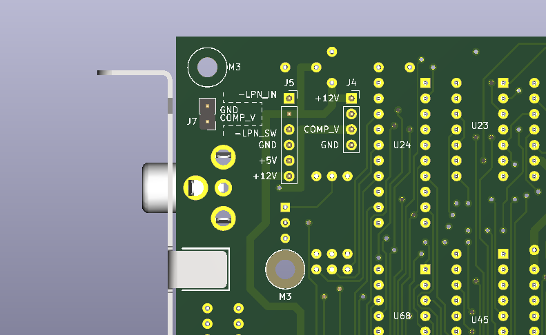
In the same spirit as the header J6, there was a desire to break out the composite video signal to a dedicated 0.1″ header, for the purposes of connecting to any future add-on cards. To that end, a two-pin header was added above the RCA jack:
The signals presented on this header (J7) are: Composite video (“CVBS”), and Ground. Note that there is already a breakout for the composite signal that comes from header J4. J7 was added anyway, in order to locate the header closer to the edge of the board and eliminate the +12v signal.
In service of mounting different add-on boards to the Retro-CGA, a series of mounting holes were added adjacent to the board bracket (under J6 and to the bottom right of the RCA jack, seen above). Three additional holes were also added nearby to the 6845 CRTC controller (H1, H2 and H3):
In theory, the holes adjacent to the CRTC controller chip could also be used as a mounting point for an FPGA-based replacement of the 6845. The addition of these mounting holes would allow for all sorts of exciting opportunities.
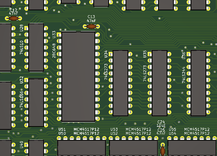
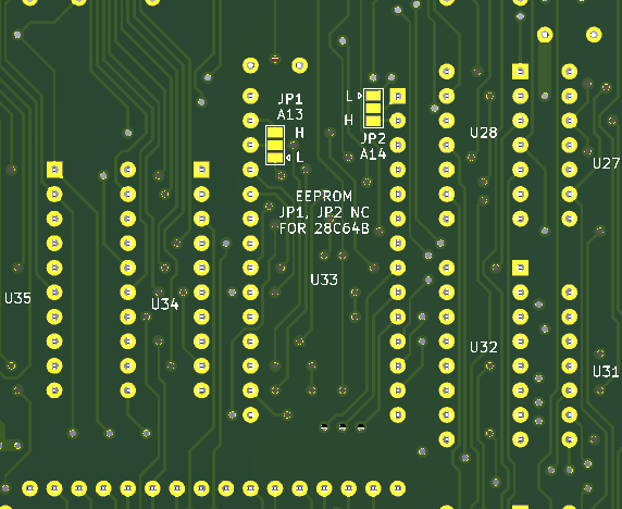
The other thing worth pointing out is the character ROM chip, which is quite large in size:
Some creative trace routing was required in order to fit this chip on the board. The board is designed around a 28C64B, but a 28C256 could also be used. In theory, a 27C64 chip would also work.
Some solder jumpers were added to the back side of the board (JP1, JP2) in order to accommodate a 28C256; the associated pins of the chip are ordinarily left unconnected for the 28C64, but can be tied low or high using these jumpers, if a 28C256 is installed. Some different character pages could be selected within the 28C256, using these jumpers, if desired:
Board Layer Detail:
Some readers may have interest in how the different layers of the board turned out. I started out trying to avoid a four-layer design, but this proved to be too difficult. Four layers were chosen in the end, in order to route some signals on internal layers. Internal signal routing was performed on the +5v internal layer.
Top layer (mixed signal):
The generation of board files in Kicad was very intuitive and easy; very similar to how Eagle PCB works. I ended up following Seeed Studio’s guide How to generate Gerber and drill files from KiCad.
The Gerbers and drill files were generated and packaged in a zip file ready for ordering online.
Depreciated Logic Chips:
One thing I hinted at in the last post was the difficulty encountered when trying to find the necessary logic chips for the Retro-CGA. As it turns out, the majority of logic chips are available, but fourteen of the ICs are types that are no longer readily produced. The special types are summarised in the table below:
| Name | Type | Notes |
| U1 | 74S112 | Used for timing generation |
| U3 | 74S86 | Used for timing generation |
| U4 | 74S174 | Used for timing generation |
| U5 | 74S174 | Used for timing generation |
| U9 | 74153 | Used for video data MUX |
| U10 | 74153 | Used for video data MUX |
| U14 | 74S32 | 74S32 on board, 74LS32 in schematic |
| U26 | 74S04 | Used for timing generation |
| U28 | 74S10 | 74S10 on board, 74LS10 in schematic |
| U29 | 74S04 | Used for timing generation |
| U31 | 74S08 | Used for timing generation |
| U43 | 74S74 | |
| U44 | 74S74 | |
| U101 | 74S174 | Used for video data MUX |
U9 and U10 raise an eyebrow straight away; they are a “74154” type, which is a part number from the very first logic family line of chips. A very early standard TTL chip (No additional letters between the “74” and the part number). This appears to be a strange choice when most other chips are 74LS series. U9 and U10 both feed into U101; they appear to act as MUX chips for the various digital video signals that feed into the RGBI video generation circuitry. The choice of “74154” type was either intentional, or a legacy detail that escaped revision over the years for whatever reason.
The other chips appear to be from the “74S” series, which is a slightly more contemporary series than U9 and U10, but still a curious choice given most other chips are 74LS series. A clue comes from the role of these chips; the majority of them are used for the generation of the various clock signals that drive different card functions. 74LS series chips may have too much gate delay to work correctly when it comes to clock generation. For example; the various NTSC colour phases would need to be timed correctly in order to function properly i.e. display somewhat accurate colour. Wikipedia implies that “74S” series chips have a typical gate delay of 3 nanosecond, compared to “74LS” series with 10 nanosecond. This difference might matter for the generation of clock signals on the card.
The “74” series and “74S” series chips proved very difficult to find online; there are of course second hand chip vendors that sell them, but I wanted to target commercially available chips for the Retro-CGA design.
The strategy going forward will be to source “74ACT” series chips, which are a contemporary CMOS design that is apparently TTL compatible. The propagation delay of the “74ACT” series is in the region of 5.5 nanoseconds, which is hopefully close enough for the purposes of the various board functions.
If the card behaves adversely, I will have to factor that in to the troubleshooting process and explore different chip types to hopefully settle on one that works.
Ordering the Boards:
There are a handful of different fabrication houses that can do 4-layer boards. In the end I chose to use PCBWay. The choice was driven largely by cost; PCBWay seemed to have the most reasonable cost considering the size and complexity of the 4-layer boards.
The exact parameters of the order were:
- Board Size: 337.82 x 106.68 mm
- Qty: 5
- Layer: 4 Layers
- Material: FR-4: TG150
- Thickness: 1.6mm
- Min Track/Spacing: 6/6mil
- Min hole size: >0.3mm
- Solder Mask: Green
- Silkscreen: White
- Gold Fingers: Yes, bevelling 20 degrees w/ 1U immersion gold
- Surface Finish: Immersion gold (ENIG)
- “HASL” to “ENIG”: No
- Via Process: Tenting
- Finished copper: 1 oz
- Add PCB product number: No
The total cost came to $208.00 USD. The board cost was $177.00, the freight was $26.00, the “bank fee” was $10.00, and I used a $5.00 off coupon.
Each of the five individual boards ended up costing $41.60
Seems like quite a lot of money in retrospect, but there would be ways to reduce this; the choice of gold fingers and immersion gold finish have likely driven the price up considerably.
Boards Inbound:
The next post in this series will cover the receipt of the prototype boards, assembly, and initial testing. Hopefully you’ve found this post interesting, and are keen to stick around to see future progress.

