In November of 2019 I taught myself how to use KiCad by practising with the creation of the ISA POST Card v2.0. It was a passable first attempt at using the software, but some annoying bugs were discovered on the circuit boards that were produced. Ever since that time I have been slowly refining the POST card design to the latest v5.1 revision. Join me for an overview of the long journey, and to finally share the design that I am happy with.
Issues with the v2.0 Design
Some errors were discovered while fabricating the v2.0 boards.
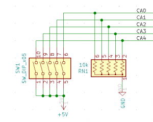
One error was accidentally swapping 5V and Ground for the address selection switches and the associated resistor networks. The overall effect was that the address selection switches operated backwards (i.e. sliding the switch upwards to the “on” position was actually selecting a logical “0” instead of a logical “1”). This was fixed by swapping 5V and Ground:
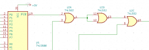
 Another major error was in the glue-logic linking the address comparator chips to the data latch chip. At the time I had used a combination of OR-gates in a 74LS32 package, not realising that the address comparator chip outputs are actually active-low. At the time, this was corrected by substituting logic elements from a 74LS02 chip (NOR-gates):
Although this substitution appeared to work at the time, there was still a deeper issue that was not resolved until many later revisions of the design, as you will see below.
The v3.1 Design
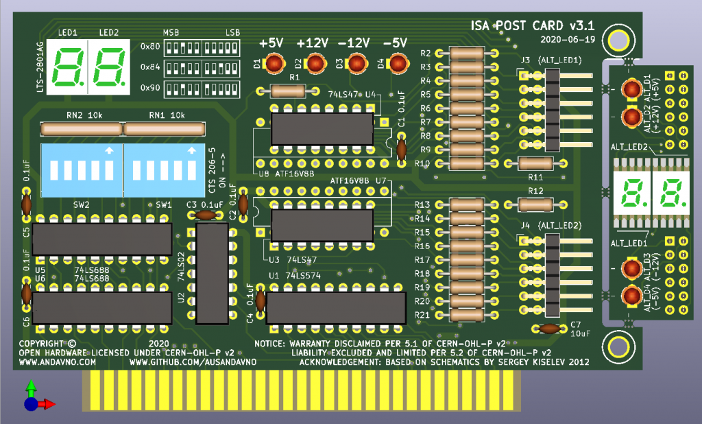
The v3.1 design was ready circa November of 2020, incorporating fixes to the various issues observed in the v2.0 design, as well as some other improvements:
Displaying Hexadecimal Values
The first and by far the biggest improvement of the v3.1 design was the inclusion of Programmable Logic Devices (PLDs) to enable the display of hexadecimal POST codes on the 7-segment displays.
The v2.0 POST card design featured two 74LS47 chips that act as BCD to 7-segment decoders/drivers. These chips are fine for displaying decimal digits from 0 to 9, but they have an obscure weakness; they cannot display hexadecimal values. Instead of displaying a hexadecimal character, they display gibberish instead. For a POST card this is less than optimal; hexadecimal values are quite common an encounter when dealing with POST codes. Unluckily for me, it was not possible to find any commercially-available chips that could do the BCD to hexadecimal conversion.
In the background, I developed a way to replicate the 74LS47 chip using an ATF16V8B PLD, and in doing so expanded the functionality such that hexadecimal POST codes could be displayed. See my post 7 segment display decoder with HEX output for more details.
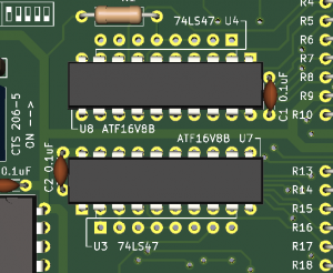
With some care assigning the PLD pins, I was able to replicate the footprint of the 74LS47 chip quite closely. The end effect was to enable the choice between either chip. If hexadecimal values were not required, the 74LS47 chip could be used. Conversely, if they were required, then the PLD chip could be substituted to enable that functionality. In order to stave off any confusion and make the distinction between the two different chip options, I offset the two footprints to overlap each other.
This was the layout with the 74LS47 chips installed:
And this was the layout with the ATF16V8B PLD chips installed:
The hope was that this optional approach would enable the best flexibility for those wishing to fabricate the board for themselves.
The one downside to this approach that I found was that KiCad DRC check would throw an error due to the different footprint courtyards overlapping. This was just shrugged off at the time; the overlapping was intentional.
Daughter Board
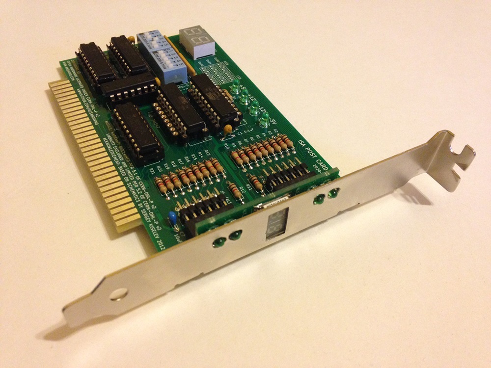
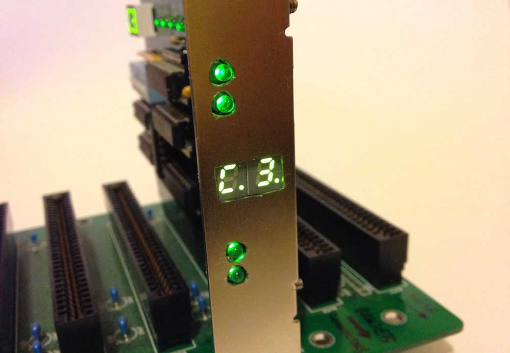
One of the “design-whims” of the v2.0 version of the POST card was the ability to view a pair of seven-segment displays through the ISA mounting bracket such that diagnostic codes could be read without opening the computer case. On the v2.0 version of the card, this was achieved via a completely separate board design.
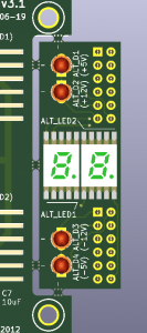
On version 3.1 of the card I wanted to try a different approach. Rather than spend time swapping between different board files, I decided to integrate a daughter-board into the main board with the use of a PCB cut-out and a series of “mouse bites”:
Using this method, only one board needed to be fabricated. If desired, the daughter-board could be snapped away from the main board and soldered together. If not desired, it could be snapped away and discarded.
At the same time as integrating the daughter-board, I decided to change the external-facing seven segment displays to a much smaller surface mount type such that they could be read horizontally.
Fabrication and Testing
The v3.1 design was fabricated around December 2020 in order to conduct some rigorous testing:
Although it did work, there were some annoyances.
I had trouble with the daughter-board approach for the smaller external-facing 7-segment displays; the PCB manufacturing house that I chose saw this as a “panellised” design and charged accordingly. I.e. they considered this to be two separate board designs joined together in a custom panel arrangement. Really not what I intended, and annoying enough to make me reconsider this approach.
I came to realise that a POST card is probably not supposed to be a permanent fixture within a computer; the ability to read POST codes through the mounting bracket may be completely redundant for troubleshooting purposes. Although it might be a fun novelty, if you are at the point of troubleshooting you are likely to have the computer case open anyway.
There was an incredibly annoying start-up behaviour; for certain combinations of 74-series logic chips installed into the board, the clock input to the data latch would sometimes trigger when powering on the machine for the first time. The first displayed value on the POST card would be either “00” or “FF” which is just patently wrong. I felt compelled to resolve this problem as it was pretty fundamental error to display values that were never on the bus to begin with.
The v4.0 Design
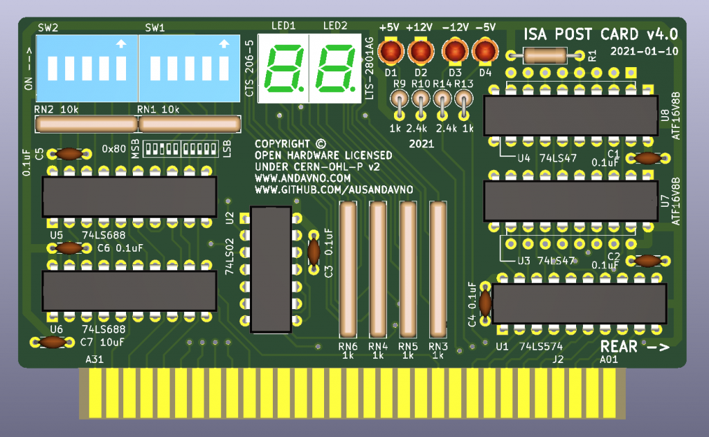
With the annoyances of the v3.1 design in mind, I set to work designing v4.0 of the card. I completed the design around January of 2021. The 4.0 version retained the Hexadecimal outputs, but completely abandoned the external-facing displays in favour of a smaller board profile (99 mm x 60 mm):
This iteration of the card was never actually fabricated or tested, as I was unable to think of a way to address the abnormal start-up behaviour without radically changing the design of the card. The v4.0 design was shelved around February 2021.
I spent the next few months analysing the v3.1 version of the card with a Logic Analyser and oscilloscope, to try and diagnose the issues at play with the abnormal start-up behaviour.
I also bought as many different varieties of the 74-series logic chips as I could (74ALSxxxx, 74HCxxxx, 74HCTxxxx, 74Fxxxx, 74ACxxxx, 74ACTxxxx, etc) in order to test different combinations of CMOS and Bipolar types.
I determined that the likely culprit was chip U2, the 74LS02 chip used as glue-logic to drive the input of the data latch chip 74LS273.
The output of chip U2 was drifting high as the board was first turned on, after which it dropped/stabilised to a ground logic level. The upward voltage drift on the output was not a lot, maybe 0.4 volts, but it seemed like it was enough to trigger a false latch and capture the data bus. Depending on which combination of 74-series logic chips I was testing (either CMOS or Bipolar series) the false latch would trap a value of either “00” or “FF”, which is what I was seeing on the seven-segment displays.
A Little Hiatus
I changed job in August of 2021, which distracted me for a few months prior to (and following) the change. I managed to pull my focus back to the POST card design again in December of 2021.
Trying to Solve the Start-up Issue
On returning to the POST card problem in December of 2021, I had a few different ideas on how to try and solve the weird start-up behaviour.
One idea was to convert all of the glue-logic chips to those with Schmitt−Trigger inputs. This was to try and avoid any partially-floating inputs from affecting the combined latch signal into the data latch chip.
The other idea was to try and implement some form of “blanking” of the 7-segment displays prior to any valid data latch signal being generated. The idea here was to blank out the display during start-up, and keep it blanked until the first (true) valid latch signal was generated. This way, it is less likely for the data latch to trap a wrong value due to its sensitivity to the input signal.
Schmitt−Trigger Inputs
I spent quite a long time trying to determine the best glue-logic chip to use that happened to have Schmitt−Trigger inputs. In the end I settled on the 74HC132, a quadruple two-input positive-NAND Schmitt−Trigger chip. The HC series was chosen more for availability than anything else, and in theory the LS series could be used instead. I could not find F, ALS or ATC versions of this chip. I would later swap to an HCT variant.
A quadruple NAND chip was chosen because it unlocked some good flexibility for construction 0f different gate types. I.e. most types of logic gate can be constructed with NAND gates as building blocks.
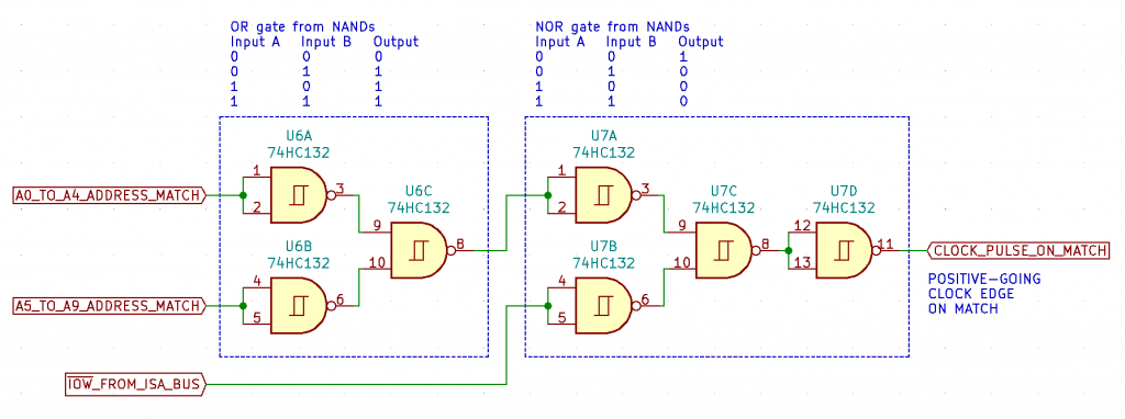
In the end I settled on the following arrangement for the glue-logic:
The two active-low match signals from each address comparator are fed through an OR gate constructed of the NANDs, with an active-low output. This active-low output is fed into a NOR gate constructed of the NANDs, along with the active-low IOW signal from the ISA bus. The output of this NOR gate is an active-high output signal that has a positive-going clock edge on address match and ISA bus write.
Keeping Displays Blanked on Start-up
The only way I could think of keeping the 7-segment displays blanked until the first (true) valid latch signal was generated was to use a D-Type positive-edge triggered flip-flop to control a “blanking” signal to be sent to either the 74LS47 or ATF16VB8 display drivers.
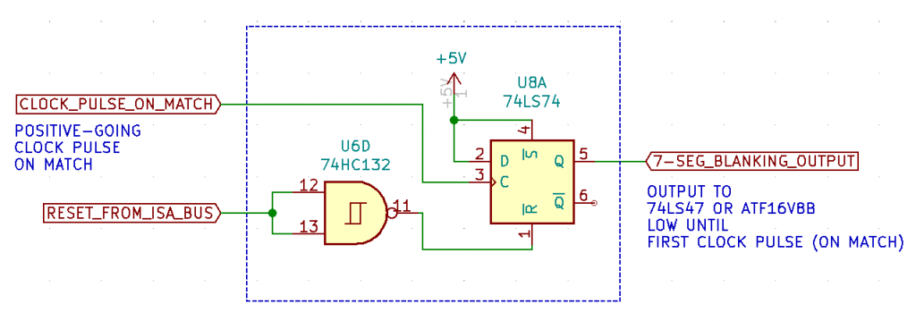
In the end I chose a 74LS74 series chip, because it had Set and Reset inputs which proved handy, and the chip was fairly easy to source. The Set input could be tied high to produce an initial low signal from the Q output of the flip-flop. The Reset input could be tied to the ISA bus Reset signal so that the POST card would behave as expected even through a “soft” computer reset.
I settled on the following arrangement:
This circuit effectively sets the flip-flop into a Toggle mode, with the initial output from Q being a low signal, until the first positive-going clock pulse on address match and ISA bus write is received, after which the output Q flips high and, in theory, the 7-segment displays are no longer blanked because their active-low inputs are no longer seeing a low signal level.
Implementing Blanking Input
The 74LS47 chips were quite easy from this point as they already had a Blanking Input pin that performed exactly as I had hoped; any logic-low signal would cause any attached 7-segment displays to show no output glyphs.
Some complexity came from the ATF16VB8 PLD chips, because they had not originally been programmed to implement the Blanking Input functionality from the 74LS47.
Quite a lot of time was spent trying to figure out how to implement Blanking Input functionality in the ATF16VB8 as the code was already close to the gate limit of the device.
Luckily I stumbled on a programming trick that allowed the Blanking Input to be implemented. See my recent article 7 segment display decoder with HEX output v2.0 (Blanking Input) for a detailed look at the required changes to the programming.
In the end I was able to implement the Blanking Input functionality within the very low gate limit of the ATF16VB8.
Ready to Revise, Again
Armed with the above designs for Schmitt−Trigger inputs, D-Type Toggle, and ATF16VB8 Blanking Input, I set to work pulling everything together into a new v5.0 design. But! I was getting very tired of spinning a new board every time the design was changed, so I took a little detour to make a certain Breadboard arrangement.
ISA Bread Board
In January of 2022 I was ready to try a new approach. Instead of endlessly spinning a new board for every trial of a design, what if… breadboard that you can plug into the ISA bus?
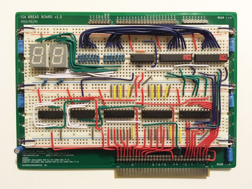
I designed this new card around two standard breadboard modules that could be stuck to its surface. The only slight difference is the use of one single power rail module between the two main prototyping modules. I could use this card to break out the ISA bus signals and allow for rapid prototyping directly with an ISA card slot. On the reverse of the card is flat space for even more breadboard modules if needed, and the common signals (address, data, IOW, IOR, Reset, etc) are grouped on a breakout on the top edge, for convenience. The holes on left and right allow for passing wires between front and back if required.
If there is any interest I can release this ISA Breadboard card as a stand-alone design.
EDIT 2023/1/29 – ISA Breadboard card has been released on Github. See recent post on this website ISA Bread Board v1.1.
Prototyping v5.0
I spent the early part of February 2022 prototyping the v5.0 design of the ISA POST card on my ISA Breadboard card:
After a bit of tweaking and adjusting, I felt I had it working correctly. On first power up, the flip-flop circuit would activate the blanking function on the 7-segment displays, until the first POST message was written to the bus at address 0x80. When the first address match was made, the flip-flop would toggle, and the blanking function was de-activated at the same time that the data bus latch was triggered. This completely eliminated the irritating start-up behaviour that I was grappling with for so long. Now, the very first code displayed is the first code received. No bogus “00” or “FF” values. The soft-reset would work perfectly by resetting the flip-flop and blanking the 7-segment displays, ready to start all over again.
After finalising the design on the Breadboard card, I moved to altering the schematics and the board design, starting from the v4.0 design that I had shelved.
v5.0 Schematic and Board Design
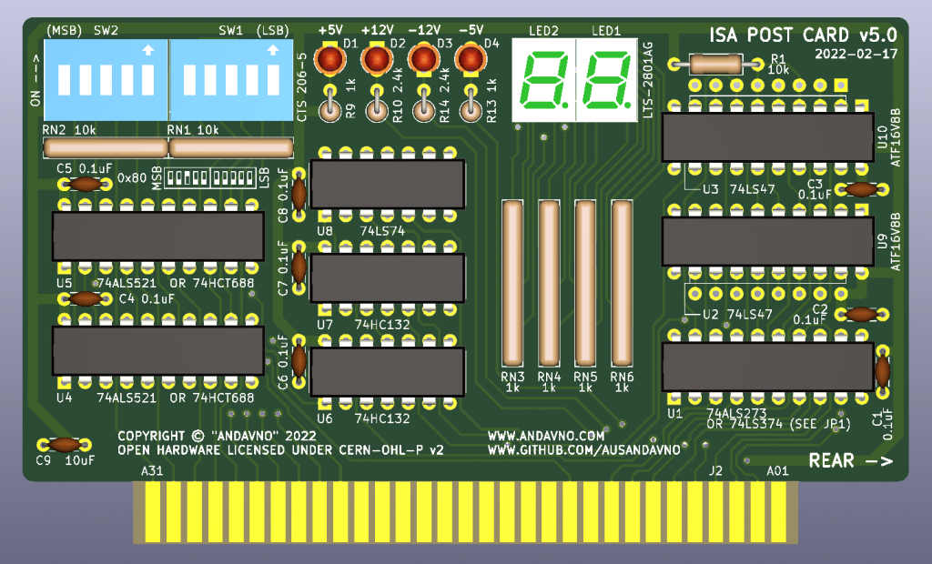
The schematic and board layout for v5.0 was finalised in mid-February 2022. Unfortunately the inclusion of more ICs resulted in slightly more board space being required. The size of the card ended up being 108 mm x 64 mm:
Compared to the v4.0 design, the locations of the 7-segment displays and the voltage indicating LEDs were swapped to make more room for the new 74HC132 chips and the 74LS74 chip.
Luckily a lot of the design work was undertaken during the Breadboard stage, so everything came together without major issue. The only complexities came from design choices resulting from supply chain disruptions.
Design for Supply Chain Disruption
One thing that was of great concern to me when prototyping the v5.0 design was the impact of supply chain disruptions that seem to be the normality around the world right now.
Many common ICs are completely sold out on Mouser or Digkey, with estimated restock times being a year or more away. Chips that usually exist in the tens of thousands are just not available for purchase.
I wanted to choose ICs that are still commonly available (for now at least!), and to give some flexibility with the use of different variants of the same functional chip, if they are available.
Luckily two different versions of the address comparator chips were found to be drop-in replacements to each other; 74ALS521 and 74HCT688.
I managed to find two close options for the data latch; 74ALS273 and 74LS374. The only difference between them is Pin 1, which needs to be tied to +5v for the 74ALS273 or tied to ground for the 74LS374. I incorporated a solder jumper for Pin 1, to allow the selection of either chip.
Tragically, as I write this, the ATF16V8B-15PU (PDIP variant) is completely out of stock at Mouser and Digikey. This only happened within the last few weeks. Back orders may be fulfilled around August of this year 2022. As a small mercy, the SOIC and TSSOP variants of the ATF16V8B are still available, so you may be able to use them with a PDIP adapter.
Although the ATF16V8B would be required to show hexadecimal values on the POST card, Sergei Kiselev has updated the BIOS for his Xi8088 and Micro8088 boards so that POST codes are only produced in decimal values I.e. he has made it so that there is no longer a need for displaying hex values. This lets the wind out of my sails a bit as I spent some effort getting the ATF16V8B to work, but it is good news from a supply chain perspective because if you intend to use this POST card in a Xi8088 or Micro8088 system you should be able to get away with using 74LS47 ICs and not notice any difference.
v5.0 Test Boards
After finalising the v5.0 design, test boards were ordered from Pcbway. The bare PCBs arrived a week or two after ordering them. They came out fairly well.
Top side of the board:
Bottom side of the board:
v5.0 Fabrication
In early March 2022 I fabricated a v5.0 board for the first time. I found it easiest to solder components onto the board in order of height, lowest to highest: Resistors (Rx), IC sockets, Resistor Networks (RNx), Capacitors (Cx), Discrete LEDs (Dx), Seven Segment LEDs (LEDx), Switches (SWx).
I populated turned-pin strip headers for U2, U3, U9 and U10. This enabled me to switch between the 74LS47 seven segment display driver IC and the ATF16V8B PLD during testing.
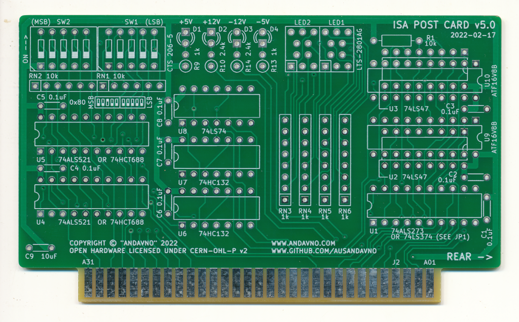
The completed board came out nicely:
v5.0 Testing
After soldering up the board for the first time, I progressed to testing.
I settled on the following default chip assignments (based on testing on the ISA Breadboard card):
U1 - 74ALS273
U2 - Not populated (74LS47)
U3 - Not populated (74LS47)
U4 - 74ALS521
U5 - 74ALS521
U6 - 74HC132
U7 - 74HC132
U8 - 74LS74
U9 - ATF16V8B
U10 - ATF16V8B
Thankfully the boards appeared to work perfectly with both of Sergey Kiselev’s Micro8088 and Xi8088.
Working with Micro8088:
Working with Xi8088:
Note that in the image above for the Xi8088, I could not actually find any record of what code A2 means; it appears briefly as part of an ascending set of codes A0 to A5, on an older BIOS version 0.9.0, pre-compiled from Sergei’s website. Unfortunately I’ve completely lost track of what the POST codes correspond to for the 0.9.0 BIOS. This may have been an artefact of the extended boot ROM in the CF card adapter that I was using.
Worried that I didn’t have a firm grasp on the range of expected POST codes that I should be seeing, I compiled Sergei’s latest BIOS version 0.9.8 for the Xi8088 and flashed it into the BIOS chip. For the Micro 8088 I kept using Sergei’s BIOS version 0.9.6.
Extended Testing with Logic Analyser
To really get an idea of what the card was doing I hooked up my Digilent Digital Discovery logic analyser to the BCD signals downstream of the data latch to check if the series of POST codes captured by the v5.0 card were at all plausible. These tests were done with the Retro-CGA card installed, and booting from a Monotech XT-CF Bootable 8-bit ISA CF interface card. For the Xi8088, the keyboard was attached. For the Micro 8088, no keyboard was attached.
Micro8088 codes (Sergei’s BIOS version 0.9.6):
#Digilent WaveForms Logic Analyzer Bus
#Device Name: DDiscovery
#Serial Number: SN:xxxxxx
#Date Time: 2022-03-23 00:13:55.245

Time (s)    Data
-6.1098277  h01
-6.1097308  h02
-6.1096628  h03
-5.6151624  h04
-5.6147422  h05
-3.7474656  h06
-3.7474466  h08
-3.6185674  h10
-3.4361687  h21
-3.4145916  h22
-3.3322741  h24
-3.2926883  h25
-3.2516277  h30
6.2779401   h31
6.3006719   h40
6.3905667   h41
6.4222303   h42
6.4235692   h43
6.4239101   h00
Xi8088 codes (Sergei’s BIOS version 0.9.8):
#Digilent WaveForms Logic Analyzer Bus
#Device Name: DDiscovery
#Serial Number: SN:xxxxxx
#Date Time: 2022-03-23 00:23:57.624

Time (s)    Data
-6.9070295  h01
-6.906933   h02
-6.9068945  h03
-6.906854   h04
-6.414398   h05
-6.413852   h06
-5.297925   h07
-5.2978855  h08
12.493376   h09
12.4934955  h10
12.4938865  h12
12.65419    h20
12.7008685  h21
12.749654   h22
12.8825445  h24
12.945755   h25
13.0496795  h30
22.573902   h31
22.6343515  h40
22.7239045  h41
22.767351   h42
22.7683345  h43
22.768517   h41
The Micro 8088 appears to completely skip code “h07” and “h09”, but I believe this may be because of the slightly older BIOS version 0.9.6. I think this BIOS was a pre-compiled version taken directly from the Micro 8088 Github page. I found it pretty hard to find consistent lists of POST codes corresponding to Sergei’s older BIOS versions. See Sergei’s errno.inc file in his “8088_bios” repository for an explanation of the meaning of the codes, at least for the latest BIOS version 0.9.8.
In testing the Xi8088 I noticed that the hexadecimal code 0xD0 would be displayed repeatedly if no keyboard was attached and the CF card adapter was taken out; I can’t really explain what this code means or why it appears.
I also noticed that the Xi8088 did not appear to reach the “h00” boot code because it would pass off to the extended BIOS in the CF card adapter and never seem to return. I may not have been waiting long enough.
Based on the testing above, I was fairly confident that the v5.0 POST card design was working as intended.
v5.1 Tweaks
Because I can’t leave well enough alone, I decided to correct some very minor issues I observed with the v5.0 board design.
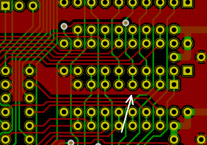
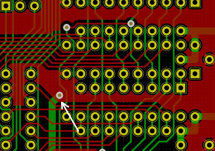
One thing that bothered me was the very thin ground-return path for chip U2 and U9. This path is also shared by one pin of one of the current-limiting resistor networks for one 7-segment display:
By re-routing some traces I was able to free up some vertical space to widen the ground-return flood fill. I also added a top-layer trace to connect downwards to a different area of the ground flood fill:
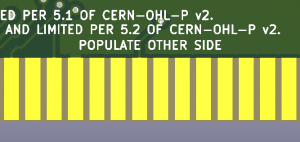
The only other thing that captured my attention was that it might not be so obvious which side of the board to populate with components; I had added rectangular boxes to the bottom silkscreen to identify the relative positions of ICs to try and help with troubleshooting. This may just be confusing if not paying attention. The fix was to add text to the top and bottom silkscreen to make it obvious which side should be populated with components.
Top side:
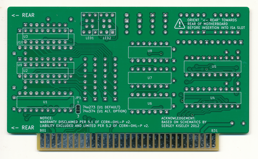
Bottom side:
One last tweak was to change the ICs for U6 and U7 from the 74HC132 type to the 74HCT132 type. The change to the HCT series was made because HCT chips have a better compatibility with TTL logic chips (I.e. bipolar type).
Because these tweaks were so minor in nature, I did not bother to print another round of PCBs to fabricate and test.
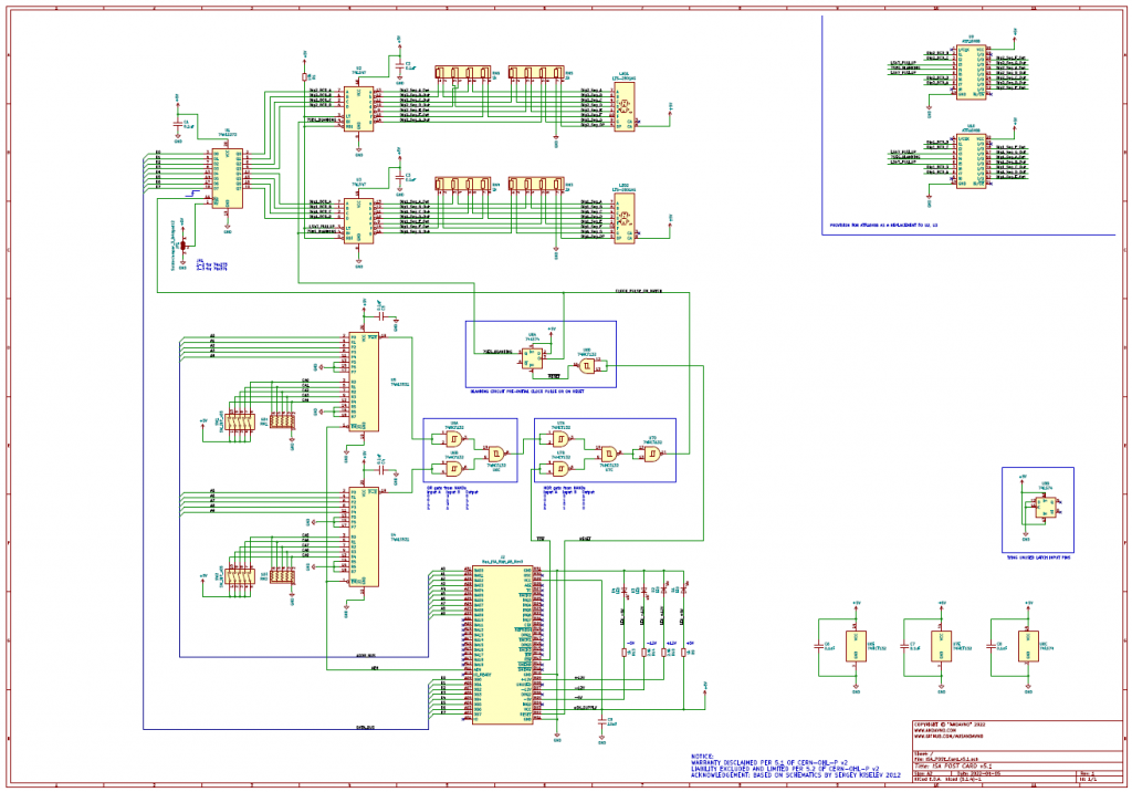
v5.1 Schematics
The schematics were updated to reflect all of the changes over the progression of the design. See my ISA_POST_Card_v5/v5.1 repository on Github to download a pdf copy (in the Schematics folder). Alternate direct link here.
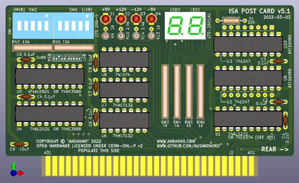
v5.1 Boards
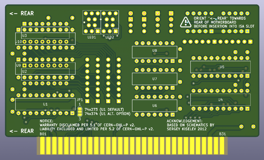
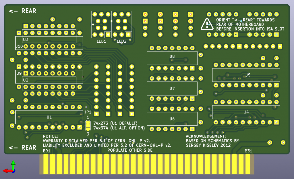
Render:
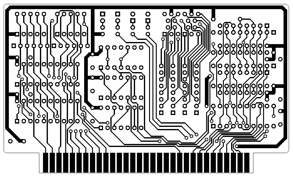
Top Copper:
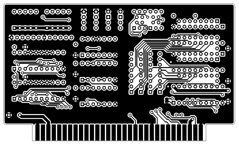
The boards were updated to reflect the small tweaks as discussed above. See my ISA_POST_Card_v5/v5.1 repository on Github to see specific board layers in pdf format (in the PCB_Layout folder).
Open Source
This will be my first attempt at releasing a design as Open Source hardware. I chose to use the “CERN Open Hardware Licence Version 2 – Permissive” model because it has been tailored specifically to hardware.
Github
Project Files (Gerbers, Schematics, KiCad files, BOM, etc) can be found in my ISA_POST_Card_v5/v5.1 repository on Github.
Conclusion
Finally! After many years of messing around, I’m finally comfortable enough to release the POST card design. I’m fairly certain the bugs have been ironed out, and I hope that it may have been worth the wait for those reading at home.
From here, I will attempt to re-focus on the Retro-CGA design. I also want to talk about another side-project that has distracted me over the last year; a solar-powered field camera for live streaming video of a bee hive.
Hoping you have found this interesting, and that you will join me on the next post.







Interested in the Prototype card with breadboard. Do you have the files for it or sell the card itself?
Hi James, thanks for showing interest in the card. I do not currently sell the card itself, but I have just uploaded all design files to my Github. See recent post https://www.andavno.com/?p=783 or direct link to Github https://github.com/ausandavno/ISA_Bread_Board_v1
how about one more little iteration? like a reset button on the board or “2pin header” for a reset. And why not put a pc speaker on it aswell? or can this be added easy somehow.
Hi Jan, do you mean a way to reset the POST card display, or a way to drive a reset signal onto the ISA bus? Resetting the post card display would be fairly easy, resetting the host machine via the ISA bus would not be possible as the host cpu typically drives the reset signal onto the bus. A PC speaker would also be difficult as they are typically driven by the host cpu. Having said that, the design is open source so you are more than welcome to experiment 🙂