Some readers may recall an older article that I wrote showing how to emulate a 7 segment display decoder with HEX output functionality, using an ATF16V8B PLD chip. The PLD programming was designed in such a way to mimic the physical characteristics of the 74LS47 BCD to 7-segment decoder/driver IC.
In progressing the belated final release of my ISA POST card design, I found myself in need of the “Blanking Input” functionality of the 74LS47 that had thus far been unimplemented in the ATF16V8B code.
This article explores the latest iteration of ATF16V8B PLD code that adds Blanking Input functionality, to better mimic the 74LS47.
Why is Blanking Input necessary?
Long story short, I have had immense trouble with start-up behaviour on more recent iterations of my POST card design.
I came very close to releasing version 3.1 of the ISA POST card in November of 2020, but I stalled in testing the card after discovering the abnormal start-up behaviour. I’m now up to version 5 of the card, with many changes from where I left off several years ago. I’m glad to say that the abnormal behaviour appears to be solved, and I’m preparing to release the latest version 5 of the card in the coming weeks/months.
In checking version 3.1 of the card for robustness, I had trialled many different combinations of 74-series logic chips, both CMOS and Bipolar type. In trialling these different types, I had found that sometimes the clock pulse into the data bus latch would float high during power-on, at least high enough to trigger a latch on the data bus that was not genuine.
What this looked like in practice was an initial POST code of “00” or “FF” when the computer is first turned on, depending on what the data bus looked like when the erroneous power-on latch occurred.
I found this unacceptable, as neither “00” nor “FF” should appear at all in the initial sequence of codes. It didn’t sit right with me that the initial code displayed could in theory be incorrect.
Blanking Input is a feature of the 74LS47 chip (as well as many others) that forces an attached display to show no value when a certain input signal is applied. For the 74LS47, when an active-low signal is applied to the Blanking Input pin, every segment of an attached 7-segment display will not be illuminated for as long as the signal is applied, regardless of the data inputs.
A Blanking Input feature should greatly expand the possible combinations of CMOS and Bipolar 74-series logic chips that could be used with my ISA POST card design, as the abnormal start-up behaviour could be masked behind the Blanking Input functionality of either the 74LS47 or an ATF16V8B PLD chip.
ATF16V8B Pin Assignment
To mimic the 74LS47 as closely as possible, the previously developed code for the ATF16V8B was modified to account for the additional Blanking Input. Pin number 4 of the 74LS47 was emulated using pin number 5 of the ATF16V8B:
How to update the ATF16V8B code
Thankfully the changes required to the previous ATF16V8B code are minimal, with some careful consideration of input pin addressing.
The first change is to add a line to the end of the Input Pin declarations in the WinCUPL project file. Pin 5 is defined as “I4”. Pin 5 is chosen as it mimics the corresponding pin location in the footprint of a 74LS47:
/* *************** INPUT PINS *********************/
PIN 8 = I0 ; /* BCD A (LSB)*/
PIN 2 = I1 ; /* BCD B */
PIN 3 = I2 ; /* BCD C */
PIN 7 = I3 ; /* BCD D (MSB)*/
PIN 5 = I4 ; /* BI */
The next change is to add “I4” to the input array definition, making sure to add it to the MSB position (left-most in array):
FIELD INPUT = [I4,I3,I2,I1,I0]; /* input array definition */
The last change is to add a row to the start of the “INPUT => OUTPUT” table definition that will catch instances of the Blanking Input pin being driven low:
['h'0..'h'F] => 'b'1111111; /* If BI active low, blank display */
This code effectively catches every input array value with a leading zero, I.e. catches the range ‘b’00000 to ‘b’01111. This means that if the blanking input (fifth bit of the input table) is zero (e.g. active-low), then every single output signal will be driven high. Remember that this code is for a Common Anode 7-segment display, so the output levels are inverted to what is expected for the segments to illuminate. An output of ‘b’1111111 is effectively turning off every segment of the Common Anode 7-segment display.
The last change is to add a “1” to the start of every discrete “INPUT => OUTPUT” table definition row, to account for the extra input signal in the fifth bit position:
'b'10000 => 'b'0000001; /* Symbol "0" */
'b'10001 => 'b'1001111; /* Symbol "1" */
etc...
The key with this implementation turned out to be the definition of an address range of ‘b’00000 to ‘b’01111 for the input table. I had initially attempted to define another sixteen rows of input spanning each new input combination, but this proved too much for WinCUPL to optimise properly. Without the slight trick of the address range definition, WinCUPL generated a solution that exceeds the available number of gates in the ATF16V8B chip.
The Final Code
See my Hex_To_Seven_Segment_Decoder (v2.0) repository on Github for the compiled “.jed” file and WinCUPL project files.
How to Compile the Code
For some instruction on how to compile the WinCUPL code for the ATF16V8B, please see “How to Compile the Code” section of my post 7 segment display decoder with HEX output.
How to Program the ATF16V8B
For some instruction on how to go about programming the ATF16V8B with a TL866II PLUS programmer, please see “Flashing U16” section of my post on building the Micro 8088.
Testing and Conclusion
After making the above changes, the newly programmed ATF16V8B chips were tested in my latest version 5 design of ISA POST card. Thankfully, they worked exactly as intended. Pin 5 can now be driven low to completely blank out the attached Common Anode 7-segment displays.
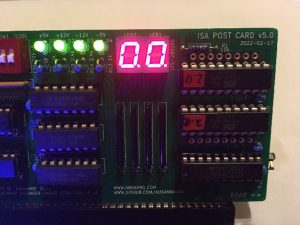
The displays in normal operation:
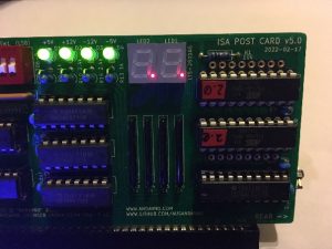
 The displays with Blanking Input signal asserted low:
Outro
I know in my last blog post I talked about how I was very close to releasing some details of the ISA POST card design, but that was in October of 2020. I did come close to releasing version 3.1 of the design in November of 2020, but the slight glitches uncovered in testing bothered me, and time has since rapidly got away from me with a background job change and all of the complications of COVID. I can at least share that I have eliminated all of the abnormal behaviour of the latest version 5 of the POST card, and I’m now more comfortable than ever in releasing it. I hope to document the way that the design has evolved and release it in the coming weeks/months. Sneak peek in the photos above.
As for the Retro-CGA, I have confirmed that the card is working and runs the 8088MPH demo. I became a little side tracked with the Retro-CGA project trying to capture the composite output of the card via an HDMI converter. I also became side-tracked with the Check-It software not displaying correctly (thinking this may have been an error with the card). The last hurdle that I am trying to overcome is an alteration of the design to use modern video RAM. I have a concept design for the use of latches to convert the CAS and RAS signals into something that a modern RAM chip would understand. Another part of me wants to just release the design as-is and worry about RAM conversion later on. I am hoping to pick a direction in the coming weeks/months and see a release through.
Hoping that you will join me again soon as I document my progress in this wonderful hobby of retro-computing.


